The Dawn of a New Semiconductor Age
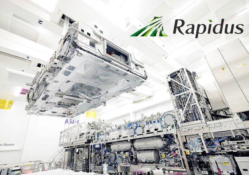
In a groundbreaking event for Japan’s semiconductor industry, Rapidus Corporation has made waves by installing it’s very first ASML NXE:3800E EUV lithography machine at its innovative integration for manufacturing (IIM-1) foundry. This exciting development took place in Chitose, Hokkaido, where the advanced semiconductor development and manufacturing fab is currently under construction.

Commemorating the Milestone
The arrival and installation of this cutting-edge EUV lithography tool was celebrated with a ceremony held at Portom Hall in the New Chitose Airport. This event not only marked the launch of superior manufacturing capabilities but also represented a significant milestone. Japan can now officially use EUV lithography technology for mass production, a feat that has been long-awaited in the realm of semiconductor innovation.
Enhancing Semiconductor Manufacturing
But the excitement doesn’t stop at the machinery installation. Rapidus is set to further boost its operations with additional state-of-the-art semiconductor manufacturing equipment. This transition aims to optimize the 2 nm generation gate-all-around (GAA) manufacturing processes, enhanced by full automated material handling systems. This integration showcases Rapidus’s commitment to leading the charge in advanced semiconductor manufacturing.
Overall, the installation of ASML’s EUV lithography equipment signals a notable shift in the semiconductor landscape in Japan, promising a future filled with technological advancements and increased production capabilities.

